Japan funds, GlobalFoundries operates: two new fabs in Malta, New York, for up to $21 billion
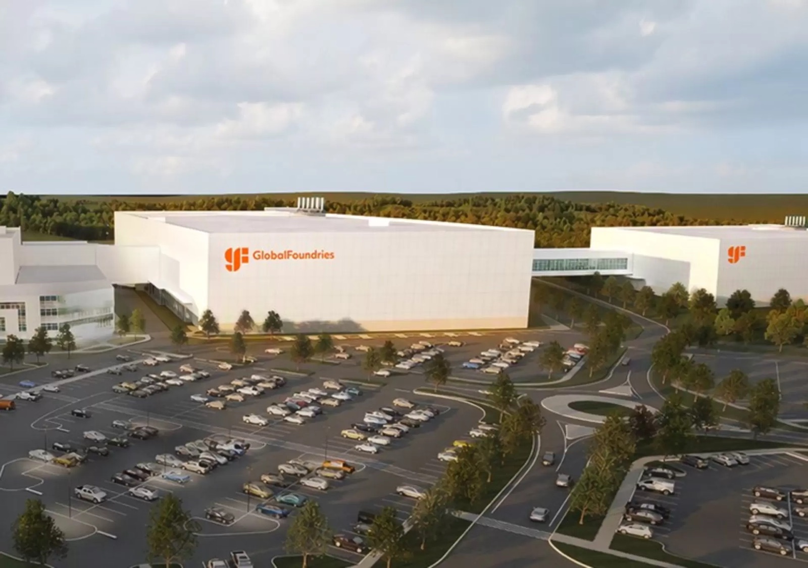
Japan provides the money, GlobalFoundries the technology
On October 14 GlobalFoundries announced it was selected as technology provider and operator for two new fabs at its Malta, New York site, under a U.S.-Japan initiative providing up to $21 billion in funding. The company said the arrangement was enabled by the trade and investment agreement between the U.S. president and Japan, and aims to accelerate trusted semiconductor manufacturing on American soil, strengthen critical supply chains and meet growing demand in automotive, industrial and connected-infrastructure markets.
The division of labour is direct: Japan supplies the investment, GlobalFoundries supplies its differentiated technologies, manufacturing expertise and operational track record as technology provider and operator. Chief executive Tim Breen framed it as fabs of this scale requiring more than capital — they require differentiated technology, operational excellence and a proven ability to execute, which he described as the combination that won GlobalFoundries the role.
The build-out comes in two steps: an initial investment of about $10 billion will accelerate construction of a new 300mm fab expected to come online in 2029, and a further $10 billion would fund a second fab. On capacity, the first fab is expected to add roughly 900,000 300mm wafers of annual U.S. capacity once fully operational, with the second adding about the same.
Employment and schedule come with concrete numbers too: the project is expected to create about 27,000 construction and ecosystem jobs plus more than 1,000 high-skilled manufacturing roles in New York's Capital Region. GlobalFoundries expects to break ground on the first fab at Malta later this year and stresses that the site is permitted and shovel-ready, letting it reuse existing Malta infrastructure to shorten construction. New York State continues to back the local semiconductor ecosystem through its Green CHIPS programme.
These are not leading-edge nodes
One positioning detail is easy to miss: these fabs target automotive, industrial and connected-infrastructure markets — so-called foundational semiconductors — rather than the smallest leading-edge logic nodes. Such chips typically use mature or specialty processes, carry modest per-unit value but ship in enormous volumes, and go through long qualification cycles. Their customers are unusually sensitive to long-term supply and to where the wafer is made: for automotive and industrial buyers, requalifying a part costs far more than any price difference.
Customer statements in the release show how that chain is composed. Renesas's chief executive said the company is planning around GlobalFoundries' new New York capacity as an extension of its own production footprint, valuing trusted U.S.-based manufacturing backed by the U.S.-Japan partnership. Equipment supplier Tokyo Electron voiced support for expanding U.S. capacity. Apple's chief operating officer noted GlobalFoundries is an inaugural member of its American Manufacturing Program, tied to a $600 billion U.S. investment commitment. Cirrus Logic said the capacity gives it domestic access for next-generation mixed-signal products, and General Motors recalled that the two companies had set up the first direct automaker-to-foundry supply agreement.
Why do automotive and industrial customers care so much about geography? Because the chip shortages of recent years rewrote procurement logic: a stalled assembly line costs far more than paying a premium to make chips somewhere more expensive. Add tariffs and geopolitical uncertainty, and having one more trusted source becomes valuable in itself, even when that source is not the cheapest.
$955 million shifted to advanced packaging, and about 4% equity for Washington
GlobalFoundries also said it agreed with the U.S. Department of Commerce to amend its existing CHIPS and Science Act award, reallocating $955 million to accelerate investments in silicon photonics, silicon-germanium and advanced packaging at its sites in Malta, New York and Burlington, Vermont. The three technologies address different demand fronts: silicon photonics and SiGe mainly serve communications and data-centre interconnect, while advanced packaging bears directly on how compute chips are assembled.
Under a separate agreement, the U.S. Department of Commerce will receive equity of approximately 4 percent in GlobalFoundries, which the company describes as letting the American public share in its growth. Subsidy in exchange for equity has become a familiar tool in U.S. industrial policy: it converts a one-off grant into an asset with upside.
Why single out packaging for redirected money? Because for AI compute chips the bottleneck is no longer only transistor density. Assembling logic chiplets with high-bandwidth memory requires silicon interposers, fine-pitch wiring, thermal management and test capacity, much of which has been concentrated in Asia. Earlier this month GlobalFoundries also announced an agreement to establish U.S.-based supply of silicon interposers for advanced AI packaging, and unveiled a roadmap for an advanced FD-SOI platform aimed at physical AI. Taken together, the three moves point at one conclusion: advanced packaging has become a strategic link in the compute supply chain.
What the news actually says
Placed in policy context: the United States passed the CHIPS and Science Act in 2022 to pull advanced manufacturing back home with subsidies, and in the years since the specific allocation of awards has kept shifting and has increasingly been bundled with equity, job commitments and supply-chain conditions. This deal's structure is unusual even so — a foreign government supplies the money, an American company operates the fabs, the capacity sits on U.S. soil, and the customers include Japanese suppliers as well as American device and car makers.
Two policy tools appear inside one transaction: a trade agreement that brings a factory onshore, and a subsidy that buys the government a stake. That says both that semiconductor capacity has become a bargaining chip in bilateral negotiations and that no single government's budget easily carries such capital-intensive projects alone.
The caveats are numerous. The $21 billion is framed as a ceiling, and the second fab still appears in the conditional — additional investment would fund it — depending on money actually arriving, permitting progress and market demand. Fabs typically take three to five years from groundbreaking to volume production, so 2029 is a target rather than a fact. And capacity aimed at mature and specialty nodes faces its own question: will automotive and industrial demand still be elevated two years from now?
For people tracking compute, leading-edge nodes and GPUs make louder headlines, but this story is about the other half of the supply chain: automotive and industrial chips, optical interconnect, silicon interposers and packaging. These links do not set peak compute, yet they decide whether the whole chain delivers on time — and GlobalFoundries is betting its position on that half.