Renesas launches the 64-bit RZ/G3L and RZ/G3SE MPUs: pin-compatible, with 1 mW-class deep standby
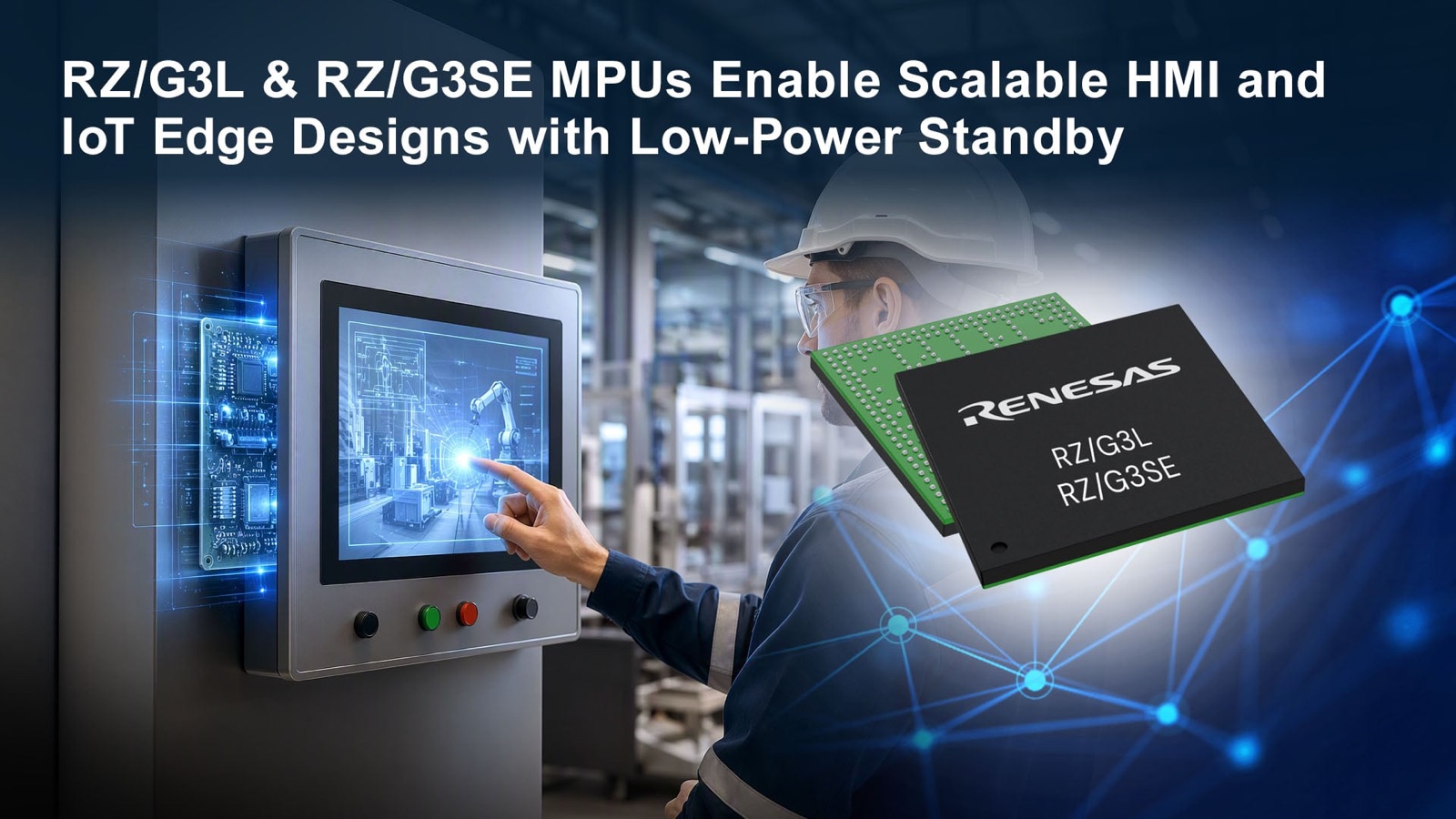
Two chips at once, and they are pin-compatible
On September 10, Renesas Electronics announced an expansion of its RZ/G Series with two 64-bit general-purpose microprocessors, the RZ/G3L and RZ/G3SE, aimed at human-machine interface (HMI) and IoT edge systems. Renesas' twist on a familiar move is the pairing: the two devices are pin-compatible, so developers can reuse one PCB design across several product lines, simplifying development and shortening time to market.
The division of labour is explicit. The RZ/G3L integrates a GPU for 3D graphics rendering along with an H.264 video codec; Renesas positions it for smart retail terminals and medical HMI devices that need both rich graphics and video handling. The RZ/G3SE drops those accelerators and targets IoT devices with basic display needs, such as EV chargers and industrial gateways that show status indicators and configuration screens. In short: inside the same package, one part is about looking good and the other about being sufficient.
Pin compatibility is a genuinely valuable property in embedded selection. The usual dilemma for an equipment maker is that a low-end and a high-end model need different hardware, which means two schematics, two boards and two rounds of certification. If the processor can be swapped up or down without a board change, one hardware design can cover several price tiers.
1 mW-class deep standby: the third-generation RZ/G power architecture
The sharpest differentiator here is standby power. Renesas says the two parts belong to its third-generation RZ/G Series, which uses a proprietary power-management architecture to bring deep-standby power down to the 1 mW level. More importantly, the Linux system stays resident in memory — the device does not have to shut everything down, so it can resume quickly when woken instead of running a full boot sequence.
That property addresses a real contradiction in always-connected equipment. Gateways, chargers and energy meters sit idle most of the time, yet must be wakeable and instantly responsive. If every wake-up requires re-booting the kernel and re-initialising peripherals, both latency and instantaneous power look bad. Keeping the system image resident while cutting power to milliwatts is a standard idea for such designs; Renesas has pushed it into the chip rather than leaving it to board-level engineering.
On the compute side the arrangement is a familiar big-little pairing: a CPU cluster of up to four Arm Cortex-A55 cores at up to 1.2 GHz, plus a Cortex-M33 co-processor running at 200 MHz. The A55s run Linux and the graphical interface, while the M33 suits control tasks with harder real-time requirements. This application-core-plus-real-time-core combination is already common in industrial and automotive designs because it separates the operating-system world from the real-time world on one die.
Connectivity, security and industrial-grade foundations
Understanding why TSN appears on parts like these means going back to what changed on the factory floor. Traditional industrial Ethernet is best-effort: when data arrives and how much it jitters depends on the load at that moment. Once a line runs motion control, vision inspection and status reporting at the same time, the control system needs to know the worst-case arrival time, not the average. TSN is a set of IEEE standards that uses time synchronisation, traffic scheduling and pre-emption to make that worst case predictable — which, for an equipment maker, decides whether one Ethernet network can carry real-time control and ordinary data together instead of running a separate fieldbus for the time-critical traffic.
On interfaces, Renesas highlights one PCIe lane, two TSN-capable Gigabit Ethernet ports and USB. The PCIe use case is spelled out: it can connect 5G modules, Wi-Fi 6 modules and even external AI accelerators. The TSN-capable Gigabit Ethernet serves industrial networks, providing the low-latency, highly reliable communication that real-time work demands.
The security and reliability configuration is the familiar automotive/industrial combination: ECC on both on-chip memory and the external DDR interface; Renesas Secure IP, secure boot, Arm TrustZone and tamper detection on the security side; and a junction-temperature range of −40°C to +125°C. Two packages are offered: a 14 mm square 400-pin LFBGA and a 17 mm square 368-pin LFBGA. On the software side Renesas provides a Verified Linux Package aligned with the Civil Infrastructure Platform (CIP), oriented toward long-term support.
In the words of Hari Pendurty, vice president of Renesas' EP Edge AI and Application Processors Business Division: as industrial and IoT devices grow more sophisticated, customers must balance performance, power consumption, connectivity and design scalability; the RZ/G3L and RZ/G3SE were developed to help them meet those changing requirements and scale products more efficiently on a common hardware platform.
Ecosystem, reference designs and availability
Renesas lists ten ecosystem solutions for the two MPUs, spanning GUI development environments, operating systems, software and system-on-modules. GUI partners include LVGL, Embedded Wizard, Slint, Candera, Spyrosoft and Qt; on the OS side it names Zephyr RTOS and Atmark Techno; on modules, Embedded Artists (a Virtium company) and Advanet. For teams using open-source GUI frameworks or Zephyr, that is a convenient signal: on the partner list at least, both toolchain and real-time system already have someone behind them.
Renesas also offers two "winning combinations": a Mode 3 AC EV charger wallbox with high-level PLC communication built on the RZ/G3L, and an AI-enabled smart home security hub built on the RZ/G3SE that integrates cameras, microphones and sensors for advanced monitoring plus cloud connectivity. Reference designs like these translate what a chip can do into what a finished product roughly looks like, which directly shapes how solution providers choose.
On availability, both devices were shipping on announcement day, and the evaluation kit — a SMARC v2.1 module board plus a carrier board — exists for both. For teams already on the RZ/G Series that means a ready upgrade path; for new projects, the evaluation cost sits in the usual range.
One caveat: neither part includes an NPU. Renesas leaves neural compute to an external path — an accelerator over PCIe, or another RZ-family device that carries an NPU. That is an explicit trade-off: in low-power, low-cost, long-lifecycle industrial and gateway designs, offloading inference to a separate part is common practice, at the price of an extra layer in both the bill of materials and the software stack.